


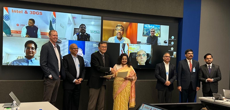
Intel Corporation and 3D Glass Solutions have signed a memorandum of understanding with the Odisha government to explore establishing an advanced semiconductor glass core packaging substrate manufacturing facility. The agreement, signed in California, aims to create a world-class facility focused on advanced semiconductor packaging technologies.
If realized, this project could be one of the largest technology investments in eastern India, potentially positioning Odisha as a hub for semiconductor manufacturing, advanced packaging, and digital technologies. The project’s success depends on regulatory approvals, funding support from the state and Central governments, and other business conditions.
India’s Ambassador to the US, Vinay Kwatra, highlighted the significance of this initiative in advancing technology cooperation between New Delhi and Washington. The proposal aligns with India’s efforts to boost domestic manufacturing and strengthen its global economic presence, according to Union Electronics and Information Technology Minister Ashwini Vaishnaw.
Odisha Chief Minister Mohan Charan Majhi sees this development as a pivotal moment for the state, aiming to transform Odisha into a competitive destination for advanced technologies, innovation, and digital transformation. The goal is to attract global technology companies, create opportunities for youth, and establish Odisha as a prominent player in the global semiconductor industry.
Babu Mandava, CEO of 3D Glass Solutions, expressed gratitude for the support from the Government of Odisha and emphasized the potential for India to become a major hub for advanced semiconductor packaging. Intel Foundry’s executive vice president, Naga Chandrasekaran, expressed pride in collaborating with 3DGS and the Odisha government, foreseeing the acceleration of next-generation advanced packaging solutions on a global scale.
