


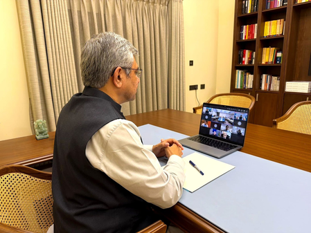
The Odisha government has partnered with Intel and 3D Glass Solutions to introduce substrate manufacturing technology in India, as announced by Union Minister for Electronics and Information Technology Ashwini Vaishnaw. This collaboration aims to enhance the semiconductor ecosystem in the country. The initiative is a part of Odisha’s broader push towards semiconductor development, with the recent establishment of the first advanced 3D chip packaging unit in Bhubaneswar.
The foundation stone for this project, under the Heterogeneous Integration Packaging Solutions initiative by 3D Glass Solutions, was laid in April at Info Valley. The project, with an investment of nearly Rs 2,000 crore, is set to produce a significant number of glass panels, assembled units, and advanced 3D heterogeneous integration modules annually. The government highlighted that Odisha is playing a crucial role in India’s semiconductor sector growth, under the leadership of Prime Minister Narendra Modi.
Union Minister Ashwini Vaishnaw praised the rapid progress of India’s semiconductor industry and acknowledged Odisha’s significant contributions. Chief Minister Mohan Charan Majhi emphasized Odisha’s unique position as the only state in India hosting both a compound semiconductor fabrication unit and a 3D glass substrate packaging facility. This development aligns with the government’s efforts to bolster the domestic semiconductor ecosystem through initiatives like the Semicon India Programme.
The Centre’s support for semiconductor projects is evident with the approval of 12 fab or packaging projects and 24 semiconductor design projects under the Semicon India Programme. Additionally, the government has introduced an online Investor Support portal to enhance investor confidence and address industry concerns effectively.
